


Antminer S11 Hash Board Repair Guide
Version date: 2019.1.26
File Category: Maintenance Plan
Content of this Volume: It mainly describes the troubleshooting of various faults of S11, and how to use the test tool for accurate positioning.
※ The copyright of this article belongs to Bitmaintech Pte.Ltd. (Bitmain). The article shall solely be reprinted, extracted or used in any other ways with the permission of the copyright owner. Please contact Bitmain official customer service if there is any need of reprinting or quoting.
I. Requirements on the Maintenance Platform
1. The constant temperature soldering iron (350-400°C). The tip soldering iron head is used for soldering chip resistors and capacitors.
2. The thermal chimney is used for chip disassembly and soldering, be careful not to heat for a long time to avoid PCB foaming.
3. APW8 power supply (output 10V—11V, 160A Max) and the power patch cord (self-produced) are used for test and measurement of the hash board.
4. The Fluke 15b+ multimeter, tweezers, V9 hash board test jig (note that some jigs do not support voltage regulation function, and cannot be used for the S11 hash board test) ((if there is condition, an oscilloscope can be configured).
5. Flux, water for cleaning panel with anhydrous alcohol; water for cleaning panel is used to clean flux residue and appearance after maintenance.
6. Tinning jig, BM1387 tin tool, solder paste; when replacing a new chip, the chip must be tinned.
7. Thermally conductive adhesive (93461) is used to re-attach the cooling fin after repair.
Tools for repairing the S11 miner are indispensable. But when your miner fails, it may also be necessary to replace some damaged parts, such as the cooling fan of the miner, the chip heat sink on the hash board, and the Antminer power cable.
II. Requirements on Maintenance Operations
1. The maintenance personnel must have certain electronic knowledge, more than one year of maintenance experience, and master QFN package welding technology.
2. After repair, the hash board must be tested twice and confirmed as OK before it can pass!
3. ay attention to the operation method when replacing the chip. After replacing any accessories, the PCB board is not obviously deformed, and the replaced parts and the surrounding area shall be checked for whether there is open and short circuit.
4. Determine the maintenance station object and the corresponding test software parameters and test jigs.
5. Check whether the tools and jigs can work normally.
III. Principle and Structure
1. Principle overview
1.1 S11 is composed of 28 voltage domains connected in series. There are 3 BM1387 chips in each voltage domain, and there are 84 BM1387 chips on the whole board.
1.2 The BM1387BF chip used by S11 is a low-voltage chip, so the power consumption of the whole miner is much improved than that of the S9 series.
1.3 The S11 clock is a 25M single crystal oscillator that is transmitted in series from the first chip to the last chip.
1.4 There is independent small cooling fin on the front and back of each chip of S11. The small cooling fin on the front side is the SMT patch, and the small cooling fin on the back side is fixed on the back of the IC by the thermally conductive adhesive after the initial measurement. After the repaired and replaced chip passes the test, it is necessary to evenly apply black thermally conductive adhesive on the IC surface and heat and fix it.
Note:
In the maintenance process, when replacing the circuit board components or the chip, in order to reduce the damage of high temperature of the blower gun to the PCB board and the chip, it is necessary to first remove the small cooling fins near the faulty component and on the back of the PCB board before replacing. There are test points on the PCB chip surfaces. When manufacturing and repairing, if there is no cooling fin attached on the PCB chip, the test point on the chip surface can be used; for repair of finished products (after-sales repair), since the front and back of the PCB are covered by cooling fins, it needs to locate fault through the test point on the chip surface of the PCB. A special slender test lead can be used to probe the cooling fin gap for measurement. However, since the SMT small cooling fin is connected to the ground of each voltage domain, it is necessary to pay attention to the insulation of the test lead in measurement to avoid short circuit caused by the test lead.
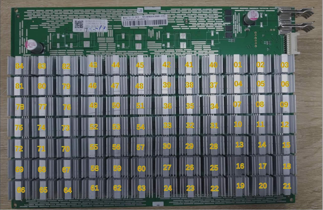
Figure 1 Signal direction
2. Analysis of key points
2.1 The following figure shows the signal direction of the S11 hash board:
The flow direction of the CLK signal is generated by Y1 25M crystal oscillator, which is transmitted from chip 01 to chip 84; during standby and computing, the voltage is 0.9V.
The TX (CI, CO) signal flows from the pin 1 at IO port the level and converts to IC, and is then transmitted from chip 01 to chip 84; when the IO line is not inserted, the voltage is 0, and the operation voltage is 1.8V when computing.
RX (RI, RO) signal flows from the 84th chip to the 28th pin of the 01th chip, and is returned to the 12th pin of the signal cable terminal control board through the level conversion IC; the voltage is 1.8V when the IO signal is not inserted, and the voltage is 1.8V during computing.
B (BI, BO) signal flows from chip 01 to chip 84 to lower the level; the voltage is 0V when IO line is not inserted and during standby, and there is a pulse signal of about 0.3 during computing.
RST signal flows from the pin 15 at the IO port, and is then transmitted from chip 01 to chip 84; the voltage is 0V when no IO signal is inserted and during standby, and 1.8V during computing.
2.2 Figure 3 shows the key circuits on the front of the S11 hash board.
2.2.1 Test points between chips (as shown below after amplified): Figure 2
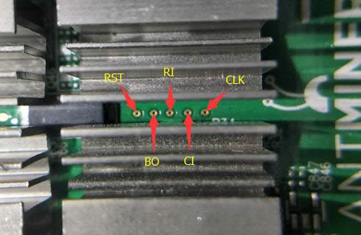
Figure 2 Test points between
During maintenance, judge the bad range roughly according to the LOG information prompted by the test fixture. The test point between the test chips is the most direct fault location method. The arrangement of the test points of the S11 hash board is:
The order of the 14 voltage domains in the 1st and 3rd rows (red box): CLK, CO(TX), RI(RX), BO, RST.
Signal:
The order of the 14 voltage domains in the 2nd and 4th rows (yellow frame) is reversed: RST, B0, RI (RX), C0 (TX), CLK.
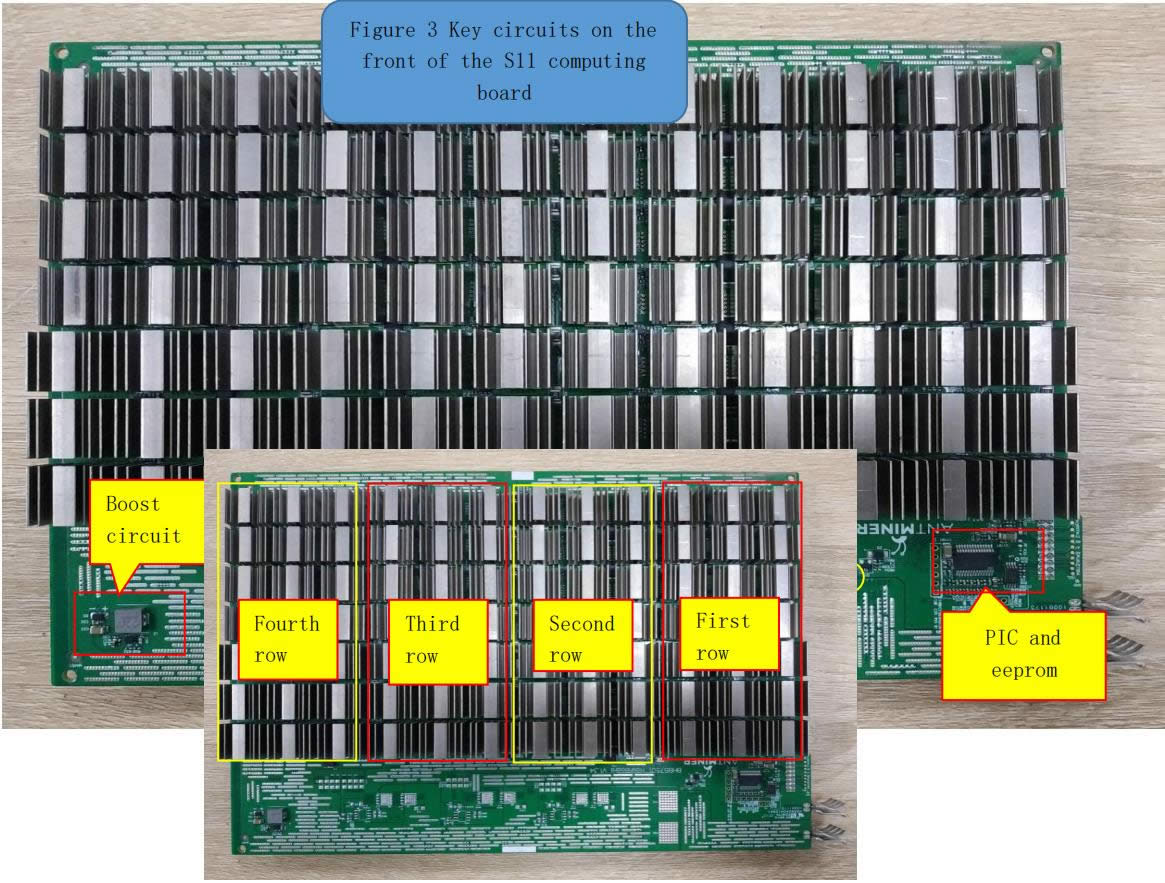
Figure 3 Key circuits on the front of the S11 hash board
2.2.2 Voltage domain
There are 28 voltage domains on the entire board, and each voltage has three chips. The three chips in the same voltage domain are powered in parallel, and are connected with other voltage domains in series after connecting in parallel. The circuit structure is shown in Figure 4 below:
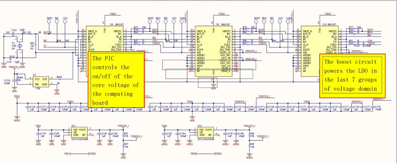
Principle analysis of single chip of voltage domain (see Figure 5 and Figure 6 below):
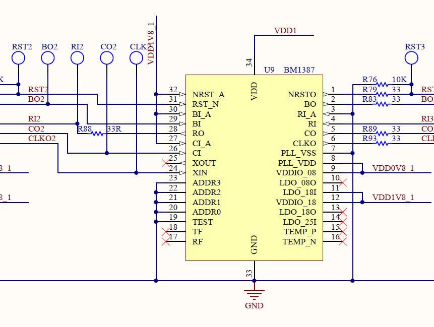
Figure 5 BM1387 circuit diagram
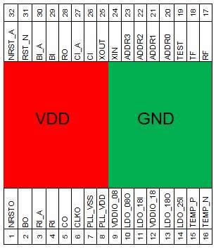
Figure 6 BM1387BF chip pin
Signal Description
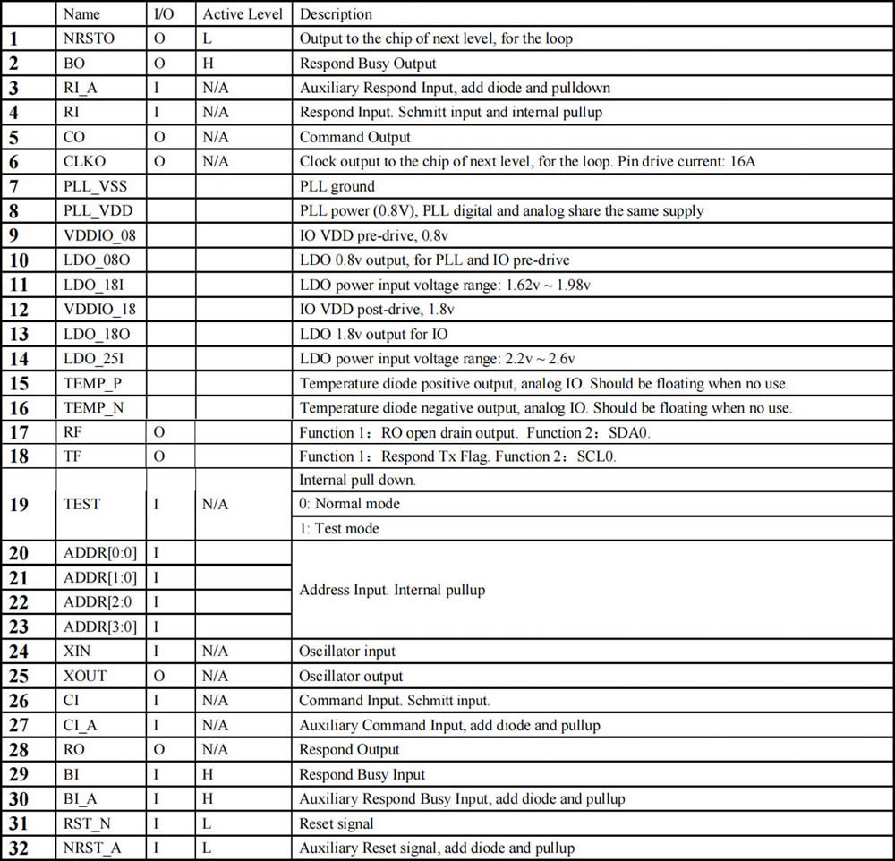
•The above is the function of each pin of the BM1387BF chip.
During maintenance, the 10 tests before and after the main test chip (five before and after the chip: CLK, CO, RI, BO, RST); CORE voltage; LDO- 1.8V, PLL-0.8V, DC-DC output, and boost 13V voltage.
Detection method:
Plug in the IO line, when the test button is not pressed, there is no voltage output in DC-DC and boost. After pressing the test button of the jig, the PIC starts to work. At this time, the DC-DC outputs the voltage set by the test program of the PIC jig, and boosts as it works. Then the jig outputs WORK, and returns to NONCE after computing. At this time, the normal voltage of each test point should be:
CLKO: 0.9V
CO: 1.6-1.8V, when the jig is just sent to WORK, since the CO is negative, the DC level will be lowered, and the instantaneous voltage is about 1.5V.
RI: 1.6-1.8V, when the voltage is abnormal or too low during computing, the hash board will be abnormal or the hashrate will be zero. BO: 0V when there is no computing, there will be a pulse jump between 0.1-0.3V during computing.
NRST: 1.8V. A reset signal is re-outputted each time the test button of the jig is pressed.
When the above-mentioned test point status or voltage is abnormal, please estimate the fault point based on the circuit before and after the test point.
•It can be seen from the above list:
CLK signal: It enters from chip 24 pin, and exits from 6 pin, when connected across voltage domains, it exits from the 6 pin and is sent to the next chip 24 pin through the 100NF capacitor.
TX signal: It enters from the chip 27 pin, and exits from 5 pin;
RX signal: It returns from the chip pin 4, and exits from 28 pin;
BO signal: It enters from chip 30 pin, and exits from 2 pin;
RST signal: It enters from the chip 32 pin and exits from 1 pin.
As shown in Figure 7 below: You can measure the signal voltage of each chip, CORE voltage, LDO-1.8O, PLL-0.8, and other voltages:
CORE: 0.4V---When this voltage is abnormal, generally the chip CORE of the voltage domain is short-circuited.
LDO-1.8: 1.8V---When this voltage is abnormal, the chip LDO-1.8O is short-circuited or open circuited, or the peripheral filter capacitor is short- circuited.
PLL-0.8: 0.8V---When this voltage is abnormal, the PLL-08 of a chip in the voltage domain is short circuited or LDO-1.8 is abnormal.
Figure 7 Test points around the chip
According to the information of the printing window of the jig, judge the operation state of the hash board, the hash rate of the chip, the temperature sense and the like.
3. IO port
IO consists of 2X9 pitch 2.0 PHSD 90-degree in-line dual row.
The definition of each pin is shown in Figure 8 below:

Figure 8 definition of each pin at IO port
As shown above:
Pin 1, 2, 9, 10, 13, 14: GND.
Pin 3, 4 (SDA, SCL): The I2C bus of DC-DC PIC, connecting the communication between the control board and the PIC. The control board can read and write the data of the PIC to control the running state of the hash board.
Pin 5 (PLUG0): The identification signal of the hash board. This signal pulls from the 10K resistor to 3.3V on the operation board. Therefore, when the IO signal is inserted, the pin should be high.
Pin 6, 7, 8 (A2, A1, A0): The EEPROM address signal.
Pin 11, 12 (TXD, RXD): Through the level conversion IC, the TX (CO) and RX (RI) signal levels of the hash board are converted from 1.8V to 3.3V of the control board.
Pin 15 (RST): It is the 3.3V terminal of the reset signal. After being divided by the resistor, it becomes a 1.8V RST reset signal.
Pin 16 (D3V3): Powers the hash board 3.3V. The 3.3V is provided by the control board, which mainly supplies the PIC with operating voltage. As shown in Figure 9 below, the voltage and distribution of each pin of IO before and after voltage division.
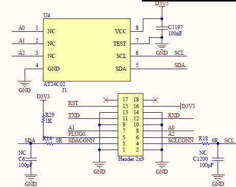
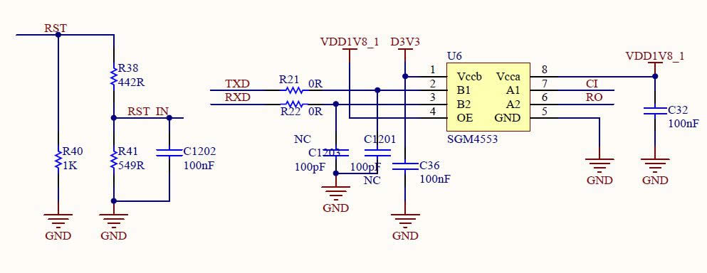
Figure 9 Voltage of the voltage divider of IO signal
4. 13V boost circuit
It is responsible for boosting DC-DC (9.8-11V) to 13V. The principle is to boost 9V voltage to 14 V through U2 SGM3750 switching power supply. The switching signal produced by U2 is the energy storage inductor through L2, and then D2 is charges and discharges the C23 to boost rectifier diode, thereby obtaining 13V of the C23 positive electrode. As shown in Figure 11 and Figure 12:
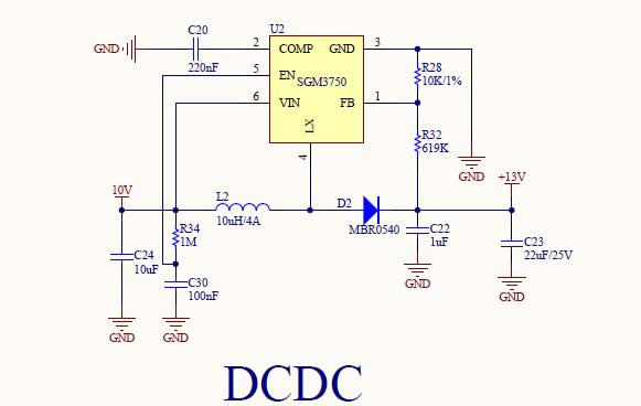
Figure 11 Schematic diagram of 13V boost
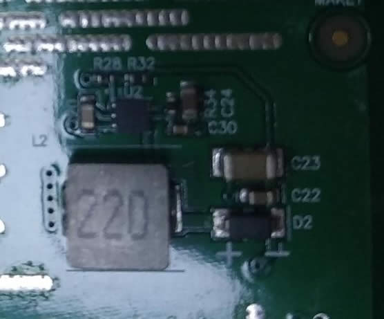
Figure 12 13V boost PCB diagram
It should be noted that the abnormal rise of the voltage of the boost circuit may easily cause damage to the LDO of the last seven voltage domains of the hash board, and may also cause chip damage.
5. DC-PIC
It consists of dsPIC33EPXXGS202_ESS and EEPROM. As shown in Figure 13 and Figure 14:
A device that stores the frequency information and temperature sensing information of the hash board chip, through which it controls the DC-DC output of the hash board.
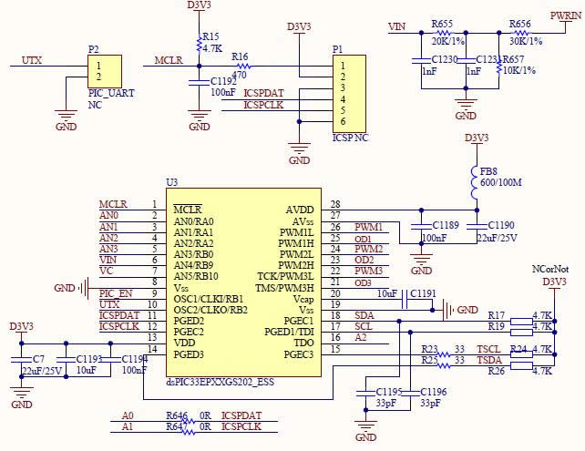
Figure 13 Schematic diagram
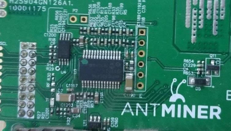
Figure 14 PIC
When the PIC is working, it needs to control and send the heartbeat signal every minute. If there is no heartbeat information, the PIC will turn off after working for one minute. PIC mainly plays the role of detecting voltage and controlling DC-DC output in the S11 board.
6. DC-DC switch circuit
It consists of 7002 and 4 CMOS tubes. When PIC_EN outputs a high level, 7002 acts as a switch, and the controlling MOS tube reaches the conducting state on as shown in Figure 15 and Figure 16:
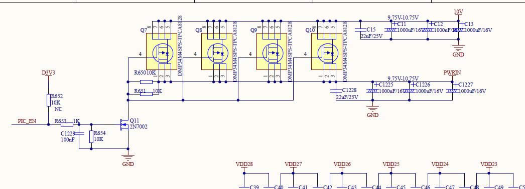
Figure 15 Schematic diagram
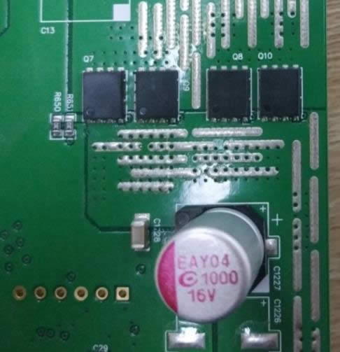
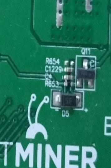
Figure 16 DC-DC switch circuit
7. 25M CLK
It consists of Y 25MHZ active crystal oscillator and 1.8V power supply: as shown in Figure 17 and Figure 18.
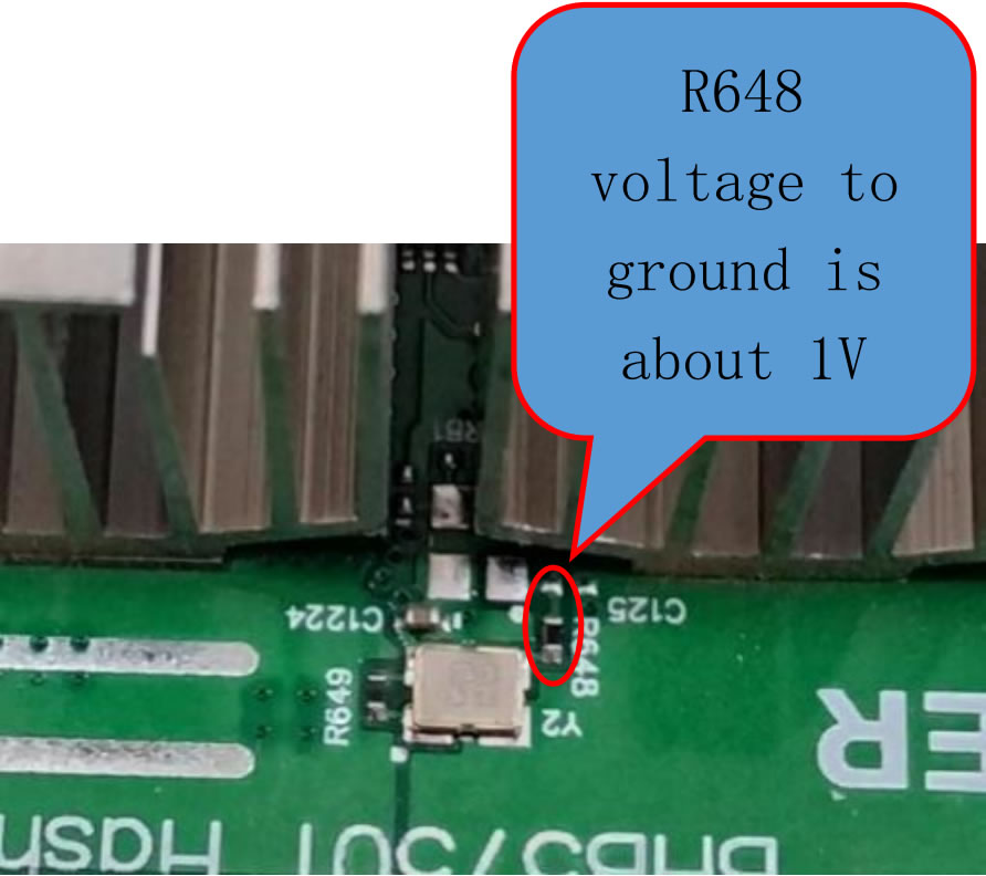
Figure 17 25M CLK circuit
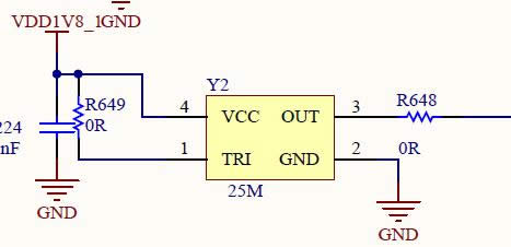
Figure 18, 25M CLK principle
Normally, the R648 voltage to ground is about 1V. As shown in Figure 19 and Figure 20 below:
The first and third pin of LN1134A18MR are inputs, and the fifth pin is 1.8V output;
It should be noted that the 1.8V LDO power supply of the last 6 voltage domains is from the 13V boost circuit; the 1.8V LDO of other voltage domains is superimposed by the CORE voltage of the last 7 voltage domains (7*0.4V=2.8 or so).
The PLL-08 voltage is obtained by dividing the LDO-1.8 by two resistors.
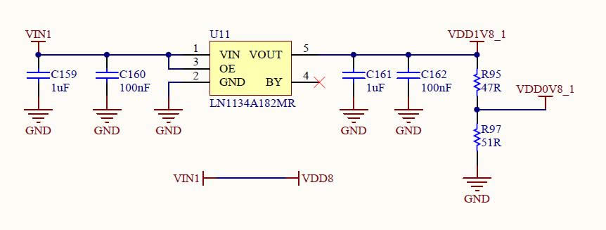
Figure 19 1.8V circuit
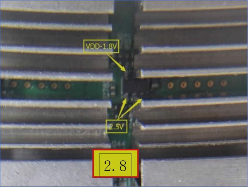
Figure 20 1.8V LDO circuit
8. Temperature sensing circuit
There are two groups of temperature sensor, one is composed of temperature sensor U5 and computing chip U39, and the other is composed of U7 and computing chip U66; the principle of each temperature sensor group: it is the built-in temperature sensor group (15th and 16th pins of BM1387) and temperature sensor, these two temperature sensing parameters are collected and finally passed the 17th and 18th pins of BM1387, and return to the FPGA of the control board through the RI. The principle is shown in Figure 21:
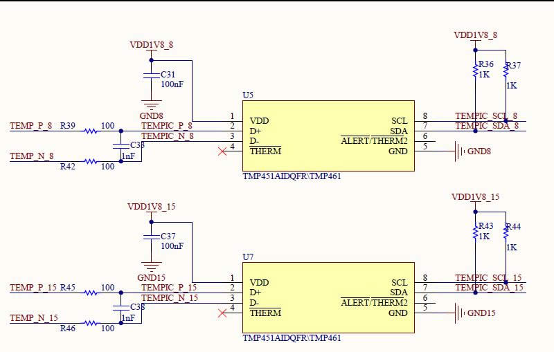
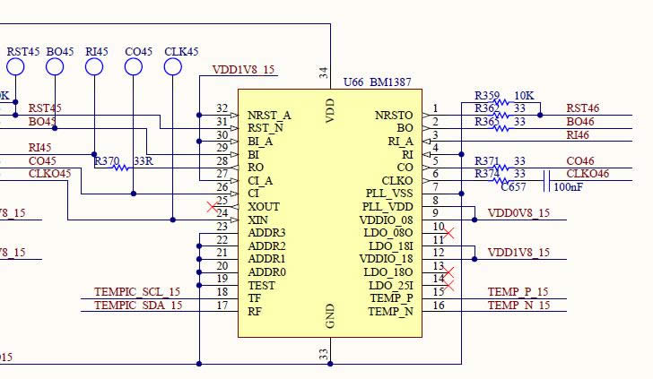
Figure 21 Schematic diagram of temperature sensing
IV. The whole miner troubleshooting
1. Log in to the monitoring interface (WEB)
Most of such faults are faults in the hash board, and a few are caused by the operating environment, fan, external network, firmware, and the like. The following are the treatments for various common phenomena:
1.1 The hashrate interface has no configuration information. As shown in Figure 22 below:
Treatment method:

Figure 22 Screenshot for no configuration information
◂ First check the indicator light of the miner. If the red light of the miner flashes, it indicates that the state of the miner is not normal. You can first check the miner network, plug in the network cable of the miner to the computer, and check whether you can ping the mining pool of the ping miner.
◂ If the state of the indicator light is normal. It is most likely that the three calculation boards of the miner have problems, and the hash board of the miner is damaged.
◂ The firmware of the miner is damaged, and the firmware can be upgraded to the latest firmware through the upgrade interface. Note that the fan is abnormal (this phenomenon can also be caused by no rotation or low speed)
1.2 No GH/S (RT) hashrate, red light flashes. As shown in Figure 23 below:
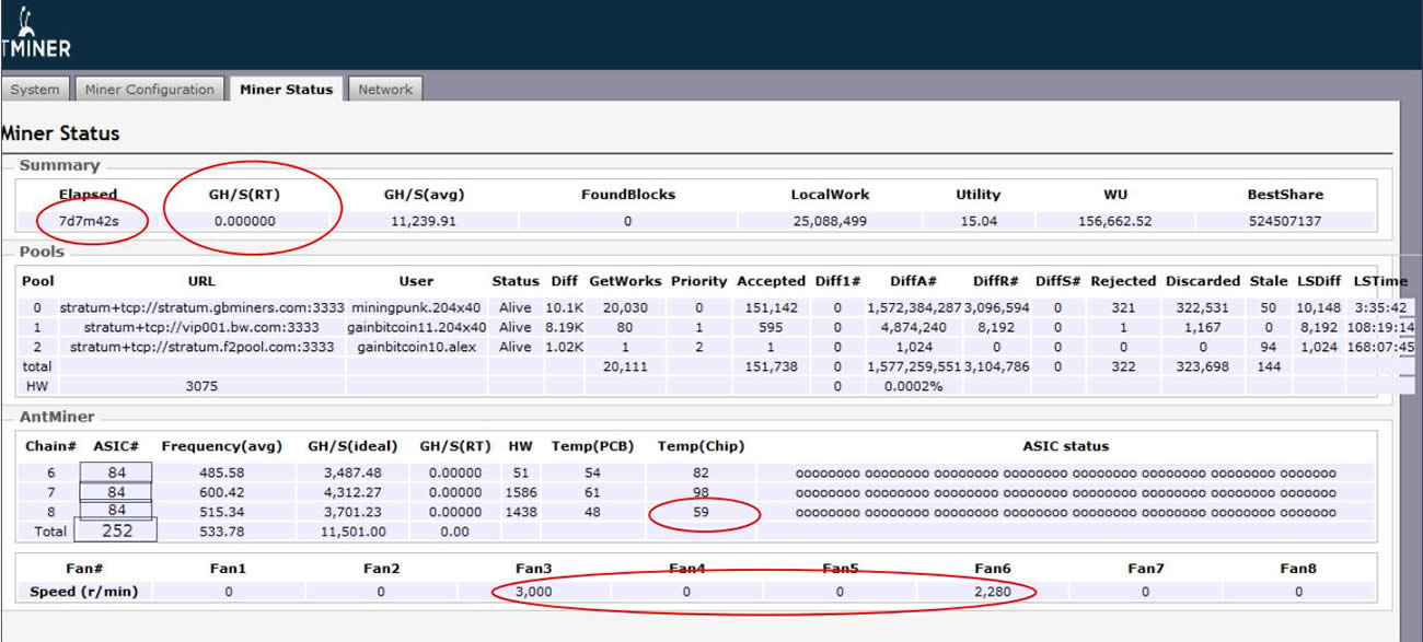
Figure 23 No real-time hashrate
In the above phenomena, the miner has been running for 7 days, and GH / S (AVG) does not drop much, indicating that the miner has not been faulty for a long time. The speed of the dual fans is very low, and the TEMP (CHIP) of the No. 8 board is very low. It is a board that has been dropped not long ago. In such phenomenon, the miner will be normal after restarting. Such phenomena have a great relationship with the operating environment of the miner, especially the ambient temperature; for example, in the winter in the north, miners are likely to have such phenomenon in case of sudden cooling.
In addition, please check if the network of the miner is connected to the mining pool? This will also happen with unstable external networks. If the system fails to operate normally after the restart, use a test tool to test the three hash boards of the miner as a single board to check whether the hash board is abnormal.
Update to the latest firmware.
1.3 Cable drops, lacks board, chip drops. As shown in Figure 24, Figure 25, Figure 26 below:
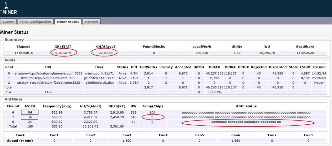
Figure 24 Chip of the hash board
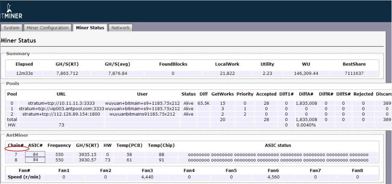
Figure 25 The miner misses one hash board
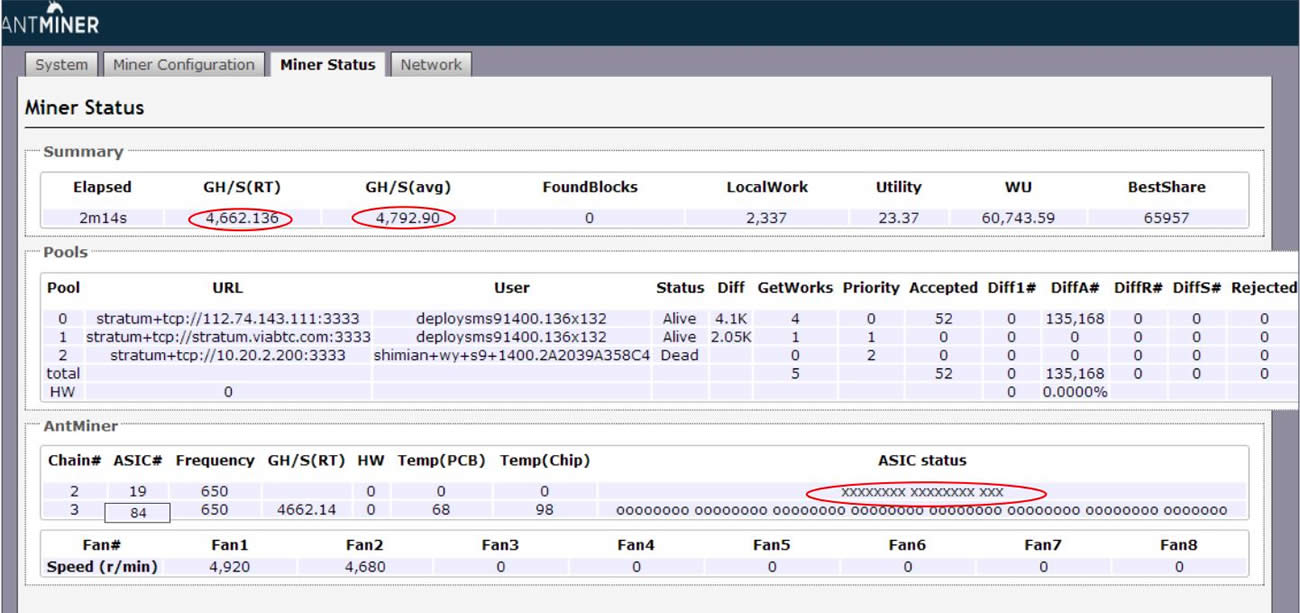
Figure 26 The miner
The above phenomenon is caused by the failure of the miner’s hash board. In Figure 23,only 34 chips are found on the 8-board hash board. Please use the jig for single-board check of the 8th board to find out the cause of the fault. In Figure 24, the 6th board can't be found. Please check the IO cable corresponding to the 6th board, and the power cord is in good contact. If there is no problem, please use the test tool for single board test of the 6th board; in Figure 25, the 1st board can't be found, and the 2nd board only has 19 chips and can't run up, please check the IO and power supply line of No.1, and use test jig for the single-board testing on the 1st and 2nd boards.
1.4 No GH/S (RT) hashrate, GH/S (AVG) hashrate reduction, chip XX phenomenon, red light flashes. As shown in Figure 27:
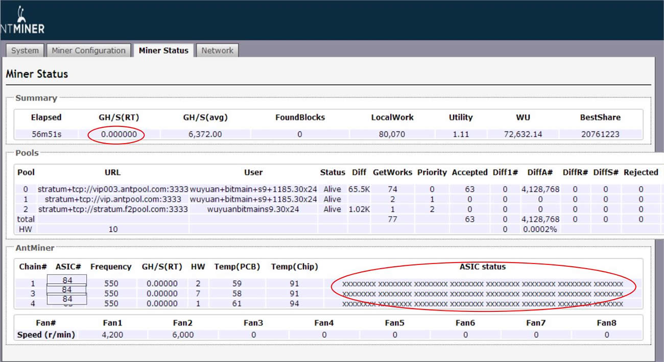
Figure 27 The chips all display XX
In the above phenomenon, GH/S (RT) is 0, GH/S (AVG) hashrate is reduced, the chips all display XX, and the red light flashes. Mostly this phenomenon is caused by abnormal operation of the control panel after the miner is disturbed. Please check the grounding of the shelf, plug-and-play mine, 220V power cord and AC-DC power supply of the miner, as well as the static electricity of the environment.
If there is no static problem and the grounding is good, please upgrade the latest firmware and use the jig for single-board test of the hash board.
1.5 No GH/S(RT), no GH/S (AVG), red light flashes. As shown in Figure 28 below
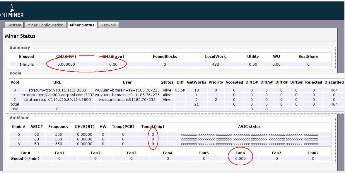
Figure 28 Only one
This phenomenon does not even have temperature. It can be seen from the above figure that only one fan is shown. The reason is that the miner only detects one fan and protects it. Please check the plug wires of the two fans, or find a normal fan to replace it.
1.6 There is GH/S (RT), GH/S (AVG) is low, and the chips all display X. As shown in Figure 29:
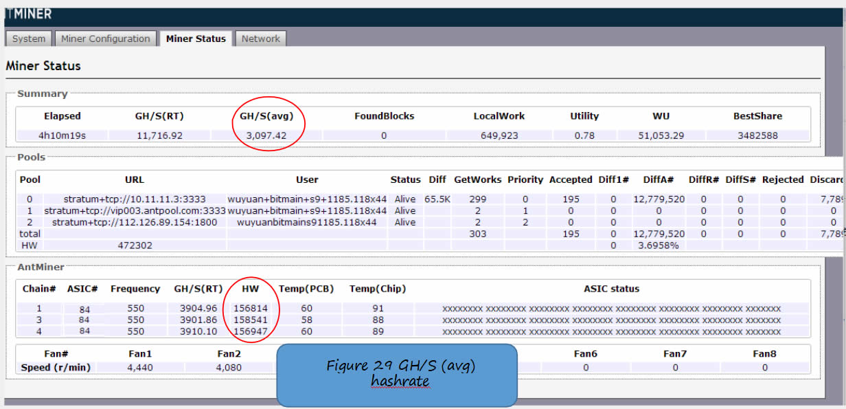
Figure 29 GH/S (avg) hashrate
Within 4 hours of operation, the HW has reached 150,000. In this phenomenon, first test each hash board with a test jig. If the hash board has no problem, please keep the updated configuration to the latest firmware.
1.7 GH/S(RT) is super high. As shown in Figure 30:
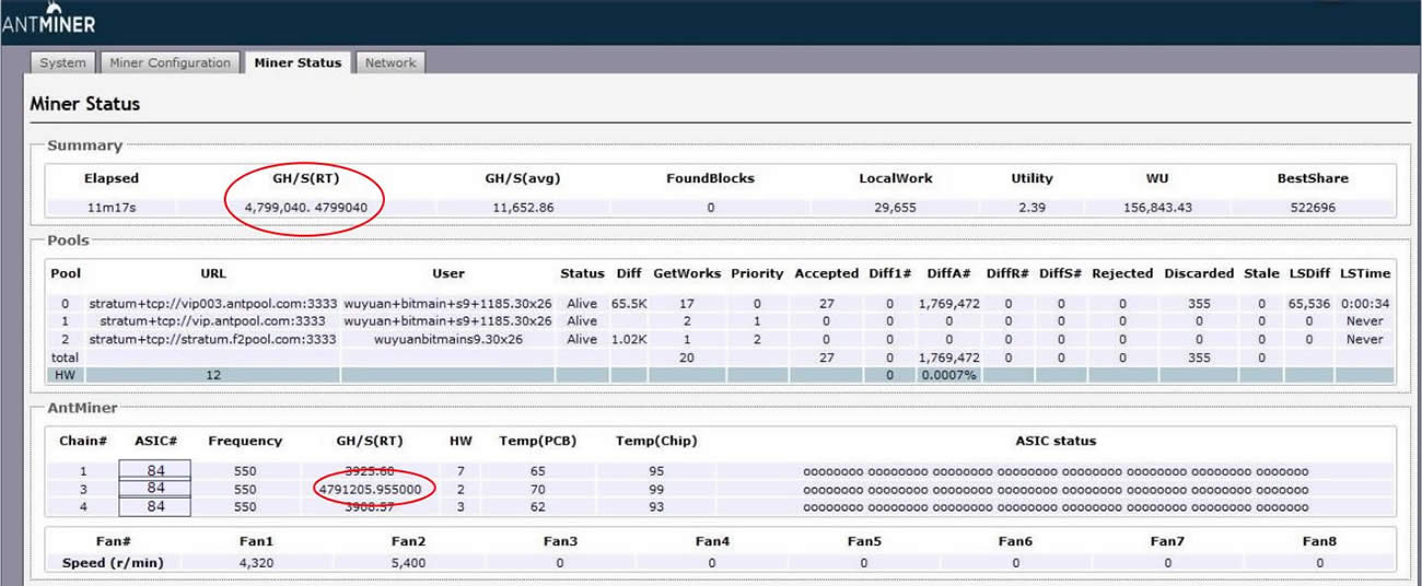
Figure 30 GH/S(avg) hashrate is high
It can be seen from the above figure that the hashrate of the No.3 board has reached 4791T. This value is definitely wrong, because some signals of the No.3 hash board are incorrect and the control board receives wrong information. Please use the test jig to conduct single-board test of the No.3 hash board. If necessary, please conduct a stress test, compare with the 550M hash board, test with 600M frequency, find the chip with a low hashrate, and then replace it.
1.8 No GH/S (RT) hashrate, red light flashes and alarms. As shown in Figure 31:
Alarm phenomenon: The ambient temperature is abnormal or the fan is abnormal. As can be seen from the above figure, the temperature of the third board has exceeded the upper limit of Temp (chip) and alarms. In this case, please check the air volume of the mine air duct. Is there any blockage in the air duct? Is the fan damaged? Is there any dust in the gap between the cooling fins?
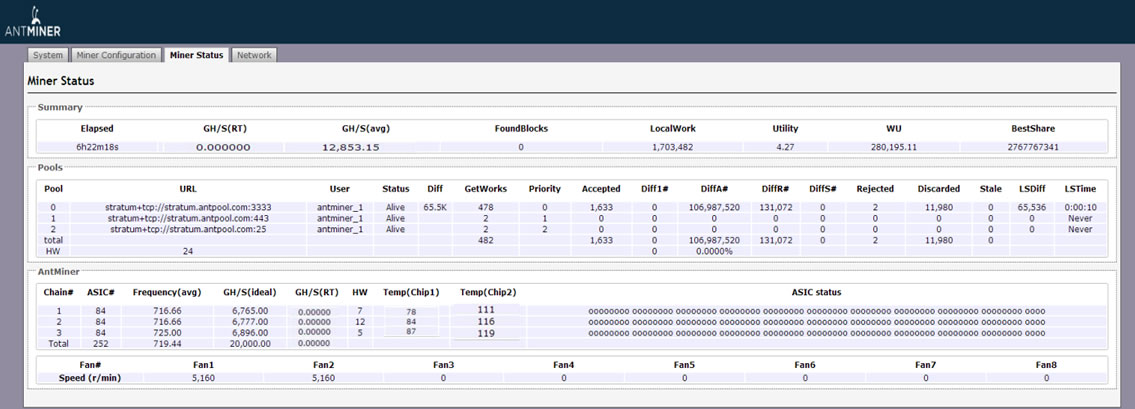
Figure 31 No GH / S (RT), the red light alarms
2. Cannot log in to the monitoring interface (WEB)
Including the failure to find the miner and IP.
Mostly the phenomena are caused by problems of the control board, especially the firmware. In this case, first restore to the factory settings to see if you can log in to the background normally, if you can, upgrade the firmware.
There are two types of control boards for the S11, and the method of restoring the factory settings is the same.
One is the Xilinx 7010 control board, as shown in Figure 32; the other is Xilinx 7007 control board, as shown in Figure 33.
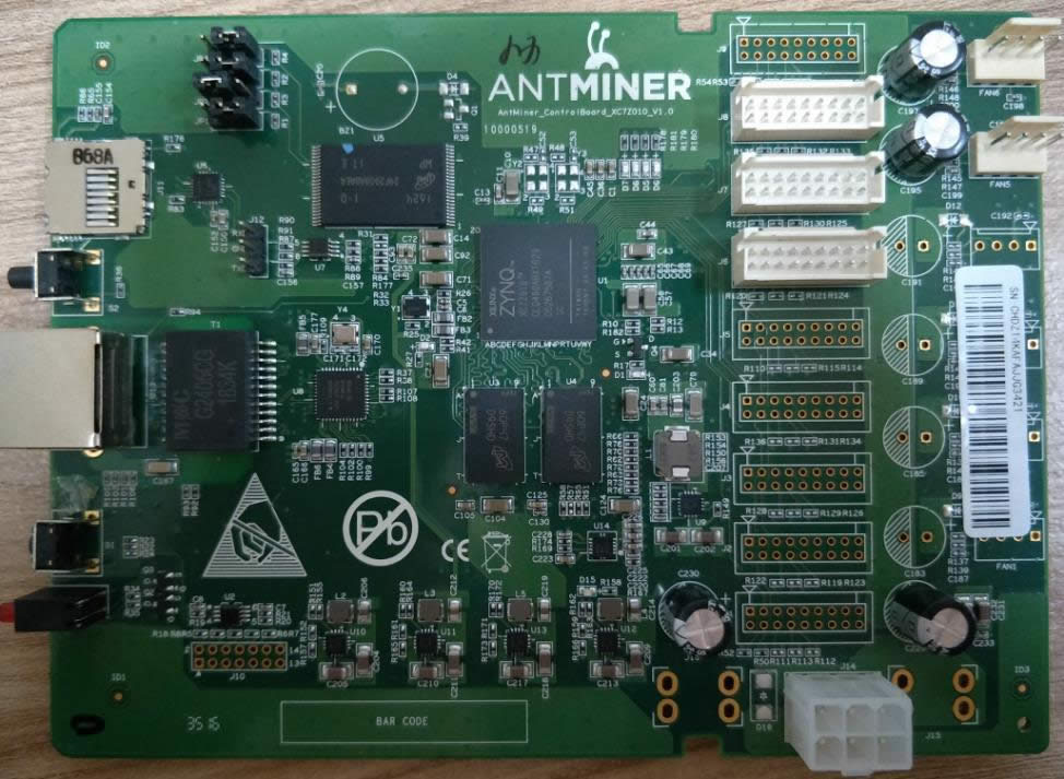
Figure 32 Xilinx7010 Control Panel
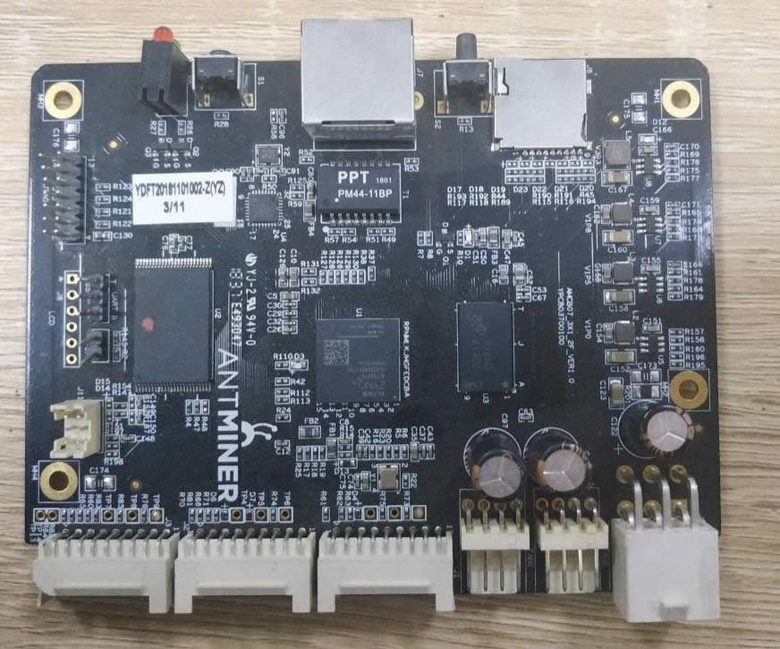
Figure 33 Xilinx7007 Control Panel
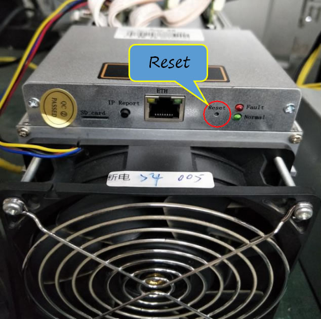
Figure 33 XILINX Control Panel
The method of restoring to the factory setting of the control panel is to press the IP Report button for 5 seconds or more when turning on, and then release when the red and green lights flash, and start to restore to the factory setting.
If the restoration to factory setting is invalid, enter the control panel maintenance process.
IV. Routine Maintenance Process

1. Routine testing: First carry out visual inspection of the hash board to be repaired to see if there is displacement, deformation, burning of small cooling fin? If there is such phenomenon, it has to be processed first; if the small cooling fin is displaced, remove it first and then clear the black adhesive, and then re-adhesive after repair.
Secondly, after it’s confirmed no problem visual inspection, the impedance of each voltage domain can be detected first to detect whether there is a short circuit or an open circuit. If found, it must be handled first.
Next, check whether the voltages in each voltage domain reach 0.4v, and the voltage difference between the voltage domains must not exceed 0.05. If the voltage in a voltage domain is too high or too low, the circuits in the adjacent voltage domain generally have abnormal phenomena, and it needs to find the reason first.
2. After confirming there is no problem in the routine test (short circuit detection is necessary in routine test to avoid burning the chip or other materials due to short circuit when it’s power-on), a test box can be used for chip detection, and the detection results of the test box can be used to judge the location.
3. According to the result of the test box detection, start from the vicinity of the faulty chip, and detect the voltage of the chip test point (CLK IN OUT/TX IN OUT/RX IN OUT/B IN OUT/RST IN OUT) and VDD VDD0V8 VDD1V8.
4. According to the signal flow direction, the RX signal is reversely transmitted (84th to 1st chip), and several of the signals CLK CO BO RST are transmitted forward (1-84), and an abnormal fault point is found through the power supply sequence.
5. When locating to the faulty chip, the chip needs to be rewelded. The method is to add a flux around the chip (preferably no-clean flux), heat the solder joints of the chip pins to a dissolved state, gently move up and down, left and right, and press the chip; promote the chip pins to joint the bonding pad again, collect the tin, so as to tin again.
If the fault is the same after re-welding, the chip can be replaced directly.
6. After the repair of the hash board, the test box must be checked for more than twice. The time of the two tests: For the first time, after replacing the parts, the hash board needs to be cooled down; after passing the test, it is put aside first. For the second time, after the hash board is completely cooled after a few minutes, the test is performed. Although each of the two tests lasts only a few minutes, it does not affect the work. The repaired board is put aside, and the second board is repaired, after the second board is repaired, it is placed and cooled, then the first board is tested. In way, the repair is staggered and there is no delay in the total length of time.
7. For the repaired board, first it is necessary to classify the faults and record the replaced part model, location, and cause, to feed back to production, after- sales, research and development.
8. After recording, install the whole miner for normal aging.
V. Fault Type
Common fault types of S11:
1. Cooling fin falls, shifts and deforms
The cooling fin on the PCB board on the back of the hash board chip is not allowed to shift or collide before power on, especially the cooling fin with different voltages. The contact of the cooling fins in different voltage domains means that there is a possibility of short circuit at different voltage points.
Moreover, determine that each of the cooling fin on the hash board has good heat conduction and is firmly fixed.
When replacing or re-installing the cooling fin, clean the residual adhesive on the cooling fin and chip and then coat again. The residual black adhesive can adjust the temperature of the blower gun to about 150 degrees and be scraped with a knife. thermally conductive adhesive can be cleaned with absolute alcohol.
2. Impedance imbalance in each voltage domain
When the impedance of some voltage domains deviates from the normal value, it indicates that there are open and short circuits in the abnormal voltage domain. Generally the chip is the most likely to cause it. But there are three chips in each voltage domain, and often only one has problem when fault occurs. The method of finding the problem chip can detect and compare the ground impedance of test points of each chip to find the abnormal point.
If there is a short circuit, first remove the cooling fin on the same voltage chip, and then observe whether the chip pin’s tin is connected.
If a short-circuit point cannot be found on the appearance, search the short-circuit point according to the resistance method or current cut-off method.
3. Voltage imbalance in voltage domain
When the voltage in some voltage domains is too high or too low, there is usually an abnormal IO signal in the abnormal voltage domain or adjacent voltage domain, which causes the next voltage domain to work abnormally and the voltage to be unbalanced. The abnormal point can be found by detecting the signal and voltage of each test point, and some need to find the abnormal point by comparing the impedance of each test point.
Note that the CLK signal and the NRST signal are the two most likely to cause a voltage imbalance.
4. Lack of chips
The lack of chips means when the test box is being checked, not all of the 84 chips are detected, and often not all the chips are actually detected. The actually lost (undetected) abnormal chips are not in the displayed position. At this time, it is necessary to accurately locate the abnormal chip through testing.
The locating method can use the TX cutoff method to find the location of the abnormal chip. That is, ground the TX signal of a chip, for example, after the tx output of the 50th chip is grounded in the voltage domain, theoretically, if all the chips in the front are normal, the test box should display that 50 chips are detected. If not all 50 chips are detected, it means that the abnormality is before the 50th chip; if 50 chips are detected, it means that the abnormal chip is after the 50th chip. Use this dichotomy to find out where the abnormal chip is located.
5. Broken chain
A broken chain is similar to lack of chips, but in a broken chain, not all chips that cannot be found are abnormal, but all the chips after the abnormal chip are invalid due to a certain chip abnormality. For example, a chip itself can work, but it will not forward other chip information; at this time, the entire signal chain will come to an abrupt end, and lose a large part of it, which is called broken chain.
Generally the broken chain can be displayed by the test box. For example, when the test box detects the chips, only 14 chips are detected. If the number of preset chips is not detected in the test box, it will not run, so it will only display how many chips are detected, at this time, according to the displayed number "14", the problem can be found by detecting the voltage and impedance of each test point before and after the 14th chip.
6. No running
No running means that the test box cannot detect the chip information of the hash board, but displays NO hash board; this phenomenon is the most common and the fault range involved is also wide.
1) No running caused by abnormal voltage in a certain voltage domain; the problem can be found by measuring the voltage in each voltage domain.
2) A chip abnormality causes an abnormality that can be found by measuring each test point signal.
CLK signal: 0.9V; the signal is output from chip 01 to chip 84. In the current version, there is only one crystal oscillator. As long as there is a signal abnormality CLK, all subsequent signals will be abnormal. Search according to the direction of signal transmission.
TX signal: 1.8V; this signal is transmitted through chips 01, 02,,,,, 84, when a certain point in the binary method is abnormal, it can be detected forward.
RX signal: 1.8V; this signal is returned from chips 84,,,,,, 02, 01, confirm the cause of the fault through the chip signal trend; when S7 and S9 hash boards do not run, the signal is the highest priority, first search for this signal.
BO signal: 0V, this signal can be lowered to high level when the chip detects that the RI return signal is normal, otherwise it is high level.
RST signal: 1.8V; after the hash board is powered and the IO signal is inserted, the signal is transmitted from 01, 02,,,,, 84 to the last chip.
3) Caused by a chip VDD
By measuring whether the potential difference between the voltage domains is normal, in general, when the VDD voltage is 0.4V, the normal voltage of each test point in other voltage domains is also 0.4V, to ensure the balance between the various voltage domains.
4) VDD1V8 voltage abnormality caused by a chip
Judge whether VDD1V8 voltage is normal by measuring the test points of each voltage. Generally, the IO voltage determines the voltage of each test point. When the IO voltage is 1.8V, the normal voltage of each test point in other voltage domains is also 1.8V
5) Caused by the abnormality of the step-down circuit and boost circuit
Directly measure whether there is voltage output (how much is the output voltage related to the jig setting) at the voltage on the two ends of C13 capacitor output in the upper left corner of the hash board. If there is no voltage output, it is necessary to confirm whether the PIC has a switching signal.
After confirming that the DC voltage is normal, check whether U2 has a voltage output of 13V, no detected peripheral parts and U2 itself.
7. Low hashrate
Low hashrate can be divided into:
1) When the test jig conducts testing, the box receives insufficient Notce, and the hashrate is insufficient and displays NG. In this phenomenon, directly judge from the number of Noce returning from each chip through the serial port print information of the test box. Generally, chips with returning Nonce number less than the set value should be trouble-checked to eliminate pseudo soldering and peripheral reason. Replace the chip directly.
2) When testing the test jig, if the hashrate is low after the miner is installed. Mostly this situation is related to the heat dissipation conditions of the chip. Special attention should be paid to the adhesive for the small cooling fin of each chip and the ventilation performance of the whole miner.
8. A chip NG
When testing through the test box, the test box’s serial port information indicates that a chip's return Nonce is insufficient or zero. In addition to eliminating the problem of pseudo soldering and peripheral components, the chip can be directly replaced.
VI. Maintenance Instructions
1. During maintenance, the maintenance personnel must be familiar with the function and flow direction of each test point, the normal voltage value and the impedance value to ground.
2. Must be familiar with the chip soldering, so as not to cause PCB foaming deformation or pin damage.
3. The BM1387 chip used by S11 cannot be mixed with S9 and T9+ (this chip is a low-power chip). 16 pins on both sides of the chip are packaged. The polarity and coordinates must be aligned during soldering and must not be misaligned.
4. When replacing the chip, the thermally conductive fixing adhesive around the chip must be cleaned to avoid secondary damage of the chip caused by hanging or poor heat dissipation during IC soldering.
● Note:
1. Since the cooling fin on the back of the chip is connected to the chip, a special slender test lead must be used to detect the test point signal; apart from the metal exposed at the contact end, the other parts of the test lead must be sealed with a heat shrinkable tube so as to prevent the test lead from contacting with the cooling fin and the test point at the same time. In particular, the voltage difference between the upper and lower rows of circuit voltage is large, and will cause damage to the chip when contacting the ground (cooling fin) and test points in different voltage domains, and special attention shall be paid.
2. In soldering, since there are small cooling gins close to the PCB on the back of the chip, the heat conduction is fast. Therefore, it is necessary to use the bottom to assist heating (about 200 degrees) in soldering, which can improve the efficiency and reduce the damage to the PCB board. If there is no bottom heating device, remove the small cooling fin on the PCB on the back of the chip before replacing the chip.
Please contact our engineering department in time for new fault types. We will analyze and update this content continuously